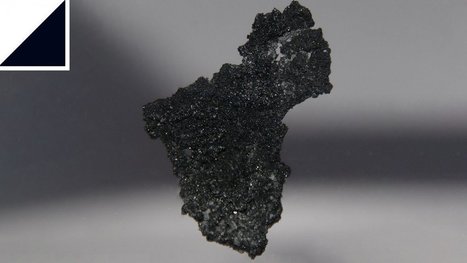
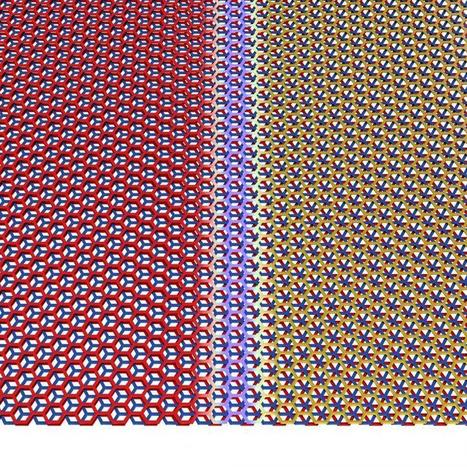
Not so long ago, graphene was the great new wonder material. A super-strong, atom-thick sheet of carbon “chicken wire,” it can form tubes, balls, and other curious shapes. And because it conducts electricity, materials scientists raised the prospect of a new era of graphene-based computer processing and a lucrative graphene chip industry to boot. The European Union invested €1 billion to kick-start a graphene industry.
Recommended for You Now Amazon plans to launch a massive constellation of more than 3,000 internet satellites Google has now cancelled its AI ethics board after a backlash from staff A new type of airplane wing that adapts midflight could change air travel Intel buys into an AI chip that can transfer data 1,000 times faster Hackers trick a Tesla into veering into the wrong lane This brave new graphene-based world has yet to materialize. But it has triggered an interest in other two-dimensional materials. And the most exciting of all is borophene: a single layer of boron atoms that form various crystalline structures.
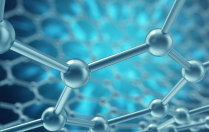
The reason for the excitement is the extraordinary range of applications that borophene looks good for. Electrochemists think borophene could become the anode material in a new generation of more powerful lithium-ion batteries. Chemists are entranced by its catalytic capabilities. And physicists are testing its abilities as a sensor to detect numerous kinds of atoms and molecules.
Not so long ago, graphene was the great new wonder material. A super-strong, atom-thick sheet of carbon “chicken wire,” it can form tubes, balls, and other curious shapes. And because it conducts electricity, materials scientists raised the prospect of a new era of graphene-based computer processing and a lucrative graphene chip industry to boot. The European Union invested €1 billion to kick-start a graphene industry.
Recommended for You Now Amazon plans to launch a massive constellation of more than 3,000 internet satellites Google has now cancelled its AI ethics board after a backlash from staff A new type of airplane wing that adapts midflight could change air travel Intel buys into an AI chip that can transfer data 1,000 times faster Hackers trick a Tesla into veering into the wrong lane This brave new graphene-based world has yet to materialize. But it has triggered an interest in other two-dimensional materials. And the most exciting of all is borophene: a single layer of boron atoms that form various crystalline structures.
The reason for the excitement is the extraordinary range of applications that borophene looks good for. Electrochemists think borophene could become the anode material in a new generation of more powerful lithium-ion batteries. Chemists are entranced by its catalytic capabilities. And physicists are testing its abilities as a sensor to detect numerous kinds of atoms and molecules.
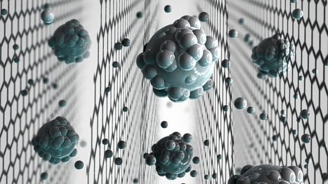
Converting CO2 into usable energy with graphene nanosheets (Nanowerk News) Imagine if carbon dioxide (CO2) could easily be converted into usable energy. Every time you breathe or drive a motor vehicle, you would produce a key ingredient for generating fuels. Like photosynthesis in plants, we could turn CO2 into molecules that are essential for day-to-day life. Now, scientists are one step closer.
Researchers at the U.S. Department of Energy's (DOE) Brookhaven National Laboratory are part of a scientific collaboration that has identified a new electrocatalyst that efficiently converts CO2 to carbon monoxide (CO), a highly energetic molecule.
Einem internationalen Forscherteam mit Beteiligung des Max-Planck-Instituts für Polymerforschung ist es gelungen, Nanotransistoren aus nur wenigen Atomen breiten Graphenbändern zu produzieren.
Forschung für die Nanotechnologie der Zukunft: Nur wenige Atome breite Graphenbänder, sogenannte Graphen-Nanoribbons, haben spezielle elektrische Eigenschaften, die sie zu viel versprechenden Kandidaten für die Nanoelektronik der Zukunft machen: Während Graphen – eine nur ein Atom dünne, bienenwabenförmige Kohlenstoffschicht – ein leitendes Material ist, kann es in Form von Nanobändern zum Halbleiter werden.
Das bedeutet, es hat eine genügend große Energie- oder Bandlücke, in der keine elektronischen Zustände möglich sind: Dadurch lässt es sich an- und abschalten – und wird so möglicherweise zu einem zentralen Bestandteil von Nanotransistoren.
Scientists have cooked up a new method for continuous production of graphene -- a process that could finally bring the exotic material out of the lab and into all the high-flying commercial applications we've been dreaming about for the past few years.
Scientists have cooked up a new method for continuous production of graphene -- a process that could finally bring the exotic material out of the lab and into all the high-flying commercial applications we've been dreaming about for the past few years.
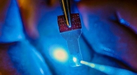
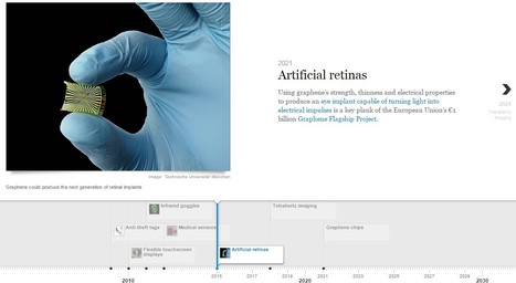
The most powerful brain implants being built today can record fast electric signals using conductive arrays while permitting light to pass out through them for high-resolution imaging . To take it up a notch, they also can let light in for optogenetic control directly under the implant. Two new studies just published in Nature Communications have the details.
The most powerful brain implants being built today can record fast electric signals using conductive arrays while permitting light to pass out through them for high-resolution imaging . To take it up a notch, they also can let light in for optogenetic control directly under the implant. Two new studies just published in Nature Communications have the details.
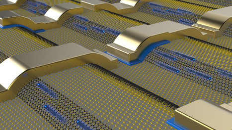
A University of Arizona-led team of physicists has discovered how to change the crystal structure of graphene, more commonly known as pencil lead, with an electric field, an important step toward the possible use of graphene in microprocessors that would be smaller and faster than current, silicon-based ...
Unlike silicon transistors used now, graphene-based transistors could be extremely thin, making the device much smaller, and since electrons move through graphene much faster than through silicon, the devices would enable faster computing.
In addition, silicon-based transistors are being manufactured to function as one of two types – p-type or n-type – whereas graphene could operate as both. This would make them cheaper to produce and more versatile in their applications.
Gust MEES's insight:
Unlike silicon transistors used now, graphene-based transistors could be extremely thin, making the device much smaller, and since electrons move through graphene much faster than through silicon, the devices would enable faster computing.
In addition, silicon-based transistors are being manufactured to function as one of two types – p-type or n-type – whereas graphene could operate as both. This would make them cheaper to produce and more versatile in their applications.
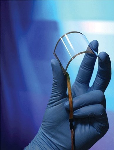
Auf diesem Material ruht die Hoffnung der Technikbranche: Graphen könnte Computer schneller, Handys flexibler und Touchscreens dünner machen. Wissenschaftler haben nun einen Weg gefunden, den hauchdünnen Stoff industriell herzustellen.
Graphene, one of the world's thinnest electronic nanomaterials, has long held the promise as a wonder material in everything from flexible touchscreens to super-fast circuits. It's that interest in semiconductors that led my team to build the world's most advanced, fully functional integrated circuit ...
Chemical and molecular engineers at at MIT and Harvard have successfully used templates made of DNA to cheaply and easily pattern graphene into nanoscale structures that could eventually be fashioned into electronic circuits.
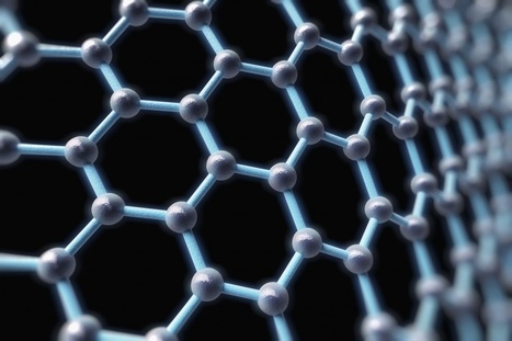
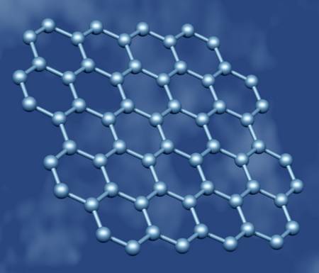
The word “super-material” gets thrown around a lot these days — ceramic super-materials, aerogel super materials, elastomeric super materials. But one super-material overshadows them all, earning its discoverers a Nobel Prize and defining the upper limit for scientific hype and excitement. It has the potential to revolutionize processing, power storage, even space exploration… but it has yet to actually achieve much of anything. It’s called graphene, and it’s the granddaddy of the modern boom in materials science. Graphene has the potential to be one of the most disruptive single inventions of all time — but what is it, really?
Scientists have been talking about graphene for the better part of a hundred years, though not always by that name. The idea was easy enough to come up with: what if we could take a diamond and slice it into wafers just one atom thick? This would make it a so-called “two-dimensional” substance, made entirely out of carbon, yet flexible in a way that diamond cannot be. It not only has the incredible physical properties you’d expect from a sheet of crystal, widely cited as the strongest material ever created on a per-weight basis, but it also has incredibly high electrical conductivity. Being atomically small, graphene could allow much, much more tight packing of transistors in a processor, for instance, and allow many electronics industries to take huge steps forward.
Kein Durst mehr auf der Welt: ein Traum, der bisher in weiter Ferne schien. Wissenschaftler haben nun ein Sieb hergestellt, das Salz aus Meerwasser filtert. Ein teurer Wunderwerkstoff macht es möglich.
Kein Durst mehr auf der Welt: ein Traum, der bisher in weiter Ferne schien. Wissenschaftler haben nun ein Sieb hergestellt, das Salz aus Meerwasser filtert. Ein teurer Wunderwerkstoff macht es möglich.
A new method of producing graphene could be the major breakthrough scientists are looking for. If the new method of producing the material on a thin polymer works at commercial scale, it could clear the way for mass production.
The potential for reproducing and adopting these graphene-like carbon nanosheets for other markets is what makes this story interesting. The team didn’t say what percent of the graphene was defect-free, but they do claim that this new manufacturing method is far simpler and less prone to failure than previous types of graphene production.
If this technique can be adapted to semiconductors or other types of solar cells, it could be far more useful than any marginal gain in organic solar cell efficiency.
According to Dr. Han Ik Joh at the Korean Institute for Science and Technology, graphene can be produced in a similar manner to carbon fiber — and while that’s hardly cheap, it’s still better than our current methods.
Learn more:
-
Gust MEES's insight:
The potential for reproducing and adopting these graphene-like carbon nanosheets for other markets is what makes this story interesting. The team didn’t say what percent of the graphene was defect-free, but they do claim that this new manufacturing method is far simpler and less prone to failure than previous types of graphene production.
If this technique can be adapted to semiconductors or other types of solar cells, it could be far more useful than any marginal gain in organic solar cell efficiency.
According to Dr. Han Ik Joh at the Korean Institute for Science and Technology, graphene can be produced in a similar manner to carbon fiber — and while that’s hardly cheap, it’s still better than our current methods.
The material has the potential to change the electronics industry, and recently researchers have focused on how to produce it commercially.
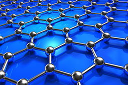
Graphene is the strongest, thinnest material known to exist. A form of carbon, it can conduct electricity and heat better than anything else. And get ready for this: It is not only the hardest material in the world, but also one of the most pliable.
Only a single atom thick, it has been called the wonder material.
Gust MEES's insight:
Graphene is the strongest, thinnest material known to exist. A form of carbon, it can conduct electricity and heat better than anything else. And get ready for this: It is not only the hardest material in the world, but also one of the most pliable.
.
Only a single atom thick, it has been called the wonder material.
The trick to this new form of graphene is that it allows electrons to act like photons. The impressive material is simply nanoribbons of epitaxial graphene—that's the honeycomb arrangement of carbon atoms you're used to seeing to illustrate graphene—that's manufactured using a relatively simple process.
The scientists grew the nanoribbons on silicone carbide wafers in which they had etched circuit patterns using standard microelectronics techniques. The silicone was then heated to about 1,000º Celsius, melting the silicone off and leaving these novel graphene nanoribbons with perfectly smooth edges. The graphene forms spontaneously on the etched edges of the silicon.
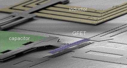
Graphene used to make world's smallest FM radio transmitter
Gust MEES's insight:
Graphene NEMS can address both problems: they are very compact and easily integrated with other types of electronics, and their frequency can be tuned over a wide range because of graphene’s tremendous mechanical strength.
Short film produced by the European Graphene-Flagship initiative, introducing graphene, the 'wonder substance' set to revolutionise the electronics industry.
Not just revolutionise the electronics industry, but many other industries, including: aviation, defence, energy, energy storage, automotive, printing and packaging; paints, coatings and barrier applications; and medicine.
Une équipe de chercheurs de l'université de Camerino (Italie), coordonnée par Andrea Perali et David Neilson, a réussi à prédire l'existence de la superfluidité à haute...
To get content containing either thought or leadership enter:
To get content containing both thought and leadership enter:
To get content containing the expression thought leadership enter:
You can enter several keywords and you can refine them whenever you want. Our suggestion engine uses more signals but entering a few keywords here will rapidly give you great content to curate.


 Your new post is loading...


April 5, 2019
Not so long ago, graphene was the great new wonder material. A super-strong, atom-thick sheet of carbon “chicken wire,” it can form tubes, balls, and other curious shapes. And because it conducts electricity, materials scientists raised the prospect of a new era of graphene-based computer processing and a lucrative graphene chip industry to boot. The European Union invested €1 billion to kick-start a graphene industry.
Recommended for You
Now Amazon plans to launch a massive constellation of more than 3,000 internet satellites
Google has now cancelled its AI ethics board after a backlash from staff
A new type of airplane wing that adapts midflight could change air travel
Intel buys into an AI chip that can transfer data 1,000 times faster
Hackers trick a Tesla into veering into the wrong lane
This brave new graphene-based world has yet to materialize. But it has triggered an interest in other two-dimensional materials. And the most exciting of all is borophene: a single layer of boron atoms that form various crystalline structures.
The reason for the excitement is the extraordinary range of applications that borophene looks good for. Electrochemists think borophene could become the anode material in a new generation of more powerful lithium-ion batteries. Chemists are entranced by its catalytic capabilities. And physicists are testing its abilities as a sensor to detect numerous kinds of atoms and molecules.
Learn more / En savoir plus / Mehr erfahren:
https://www.scoop.it/t/21st-century-innovative-technologies-and-developments/?&tag=Graphene
https://www.scoop.it/topic/21st-century-innovative-technologies-and-developments/?&tag=Research